Epitaxial nanostructures
The research group semiconductor epitaxy produces and studies semiconductor and metal heterostructures with tailored optical, electrical and magnetic properties. Carriers are confined in these systems in artificial potentials at the nanoscale. This makes it possible to reveal the quantum nature of the systems and to design new ways of controlling and applying their unique properties.
Semiconductor layers with extremely high purity are deposited in solid source molecular beam epitaxy (MBE) systems. Composition of the layers and their thicknesses are controlled with atomic accuracy. Such semiconductor heterostructures are of great interest for technological applications. They form the basis of many modern semiconductor devices such as lasers and quantum well transistors with heterojunctions. On the other hand, many basic research questions in solid state physics are elucidated experimentally using special heterostructure devices. The precise control of chemical composition, doping and layer thicknesses using the MBE and the lateral patterning by lithographic methods or self-organization effects enables the production of low-dimensional electron systems and artificial potential gradients, in which quantum effects play a central role.
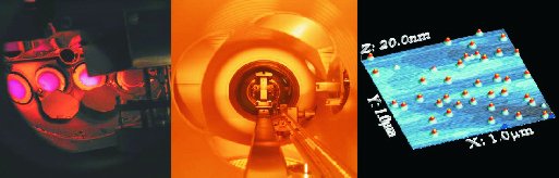
Left: View of a MBE growth chamber. Clearly visible are the red-hot crucibles located inside of the effusion cells. The elementary epitaxial material is located inside of the crucibles. Middle: Inner view of a UHV transfer chamber of the MBE cluster. It contains a transport system to transport samples from one chamber of the cluster to another. Right: AFM image of MBE-grown self-assembled InAs quantum dots on a GaAs (100) crystal surface.
An ultra high vacuum (UHV) cluster is built inside of the semiconductor epitaxy lab. The cluster is equipped with two Riber and a metal-epitaxy growth chambers. A growth chamber (Riber 32P) was installed in 1997 and is currently equipped with group III elements such as indium, gallium, aluminum and arsenic as a Group V element. For doping with donors or acceptors in each case a silicon cell and a carbon-cell are installed. Also located for producing semi-magnetic III-V semiconductors, a manganese-cell in the growth chamber. The second growth chamber (Riber C21) is optimized for high-mobility heterostructure transistors. It is currently equipped with indium, gallium, aluminum and arsenic-cells as well as a silicon doping cell. The cluster also contains a process chamber for the pretreatment of the substrates. A UHV-STM chamber for analysis and manipulation of the epitaxial films with scanning probe methods are currently under construction.
The fundamental properties of products made with exceptional modulation doping quasi-free two-, one-and zero-dimensional carrier systems are investigated by magnetotransport experiments. For such experiments are cryostat with superconducting magnet and testers for high-resolution capacitance spectroscopy, admittance spectroscopy, deep level transient Spectroscopy and Hall-effect measurement spaces. In addition, a (3He/4He) dilution refrigerator is maintained by the research group, which is suitable for measurements at low temperatures down to 20 mK and in magnetic fields up to 16 T in order to make even weak quantum effects measurable. Furthermore, an atomic force microscope is used to elucidate the structure of the crystal surfaces.
In future-oriented concepts are quantum wires and dots represent the fundamental units, such as qubits for quantum computers or switch spinning and spinning pumps for spintronics. Quantum dots are artificial atoms as already used for single photon emitters and laser applications in communication technology and quantum wires as electron waveguides in research laboratories for specialized applications such as highly sensitive electrometer, and spin filter. Currently, the biggest challenge of the basic elements of more complex to build functional molecule-like structures and to explore their properties.
For producing the structures we apply both conventional methods of semiconductor technology as well as novel methods based on self-organizing mechanisms or some in which we use scanning probe microscopes. If, for example, InAs is epitaxially deposited on GaAs , strain driven InAs droplets arise on the surface of GaAs matrix. These structure form nanometer-sized quantum dots with unique electrical and optical properties. In addition to studying the structural and electronic properties, we develop methods by which we can determine the location of the nucleation of these so-called self-organized quantum dots.
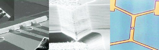
Left: Curved lamella with semiconductor contacts for measurements of the magnetoresistance. Light gray areas are metal strips forming electrical contacts to the electron system. Middle: Detached wire bridges, the gate electrode of a component for highly sensitive contact capacitance measurements. Right: GaInAs heterostructure device which contains an electron billiards with 1 micron distance between two two-dimensional electron systems.
A key research focus of the working group concerned with InAs containing heterostructures. Two important features distinguish InAs in addition to the low band gap: The conduction band electrons in the material feel a very strong spin-orbit coupling and metal-semiconductor contacts on the media have a negligible Schottky barrier. Because of these properties, the material is promising for applications in novel spintronic devices. We produce InAs-based heterostructure metamorphic transistors on GaAs substrates with high mobility and study the effect of spin orbit coupling on the transport properties of heterostructure transistors.
Apart from the formation of the self-assembled quantum dots, the strain accumulated in GaAs-InAs heterostructures can be applied for production of electron systems in curved planes. Free-standing, curved epitaxial films are made by selective etching an underlying sacrificial layer. Novel systems such as semiconductor rings, optical resonators in micrometer sizes, nano-rolls, and the quantum wells comprise a two-dimensional system, are investigated. Detached layers that are only a few nanometers thick, it is easy to bend due to thermal expansion or mechanical application of electric fields. Novel applications of such structures as detectors and actuators are investigated.