Main fields of interest of Christian Heyn
Structural and optoelectronic properties of self-assembled semiconductor nanostructures
We fabricate heterostructures composed of III/V-compound-semiconductors by using solid-source molecular beam epitaxy (MBE). Beyond classical heterostructures comprising a stack of plane layers, nanostructures with a three–dimensional confinement for charge carriers are realized by utilizing self-assembly mechanisms. The most prominent example for such self-assembled nanostructures are strain-induced InAs quantum dots (QDs) grown in the so called Stranski-Krastanov mode (Fig. 1a). The driving force for QD generation in Stranski-Krastanov mode is the minimization of the strain energy caused by the lattice mismatch between the InAs deposit and the GaAs substrate. An alternative technique for QD self-assembly is the droplet epitaxy in Volmer-Weber mode which is more flexible regarding the choice of the materials (Fig. 1b). During droplet epitaxy, the liquid droplets are crystallized into semiconductor nanostructures. On the other hand, using modified process parameters, the droplets behave completely different and perform a local removal of substrate material. This local droplet etching (LDE) represents a very powerful technique allowing the self-assembled patterning of semiconductor surfaces without any lithographic steps (Fig. 1c). The LDE nanoholes are surrounded by distinct walls that may act a quantum rings (Fig. 1d). Furthermore, strain-free and highly uniform QDs are fabricated by filling of the nanoholes.
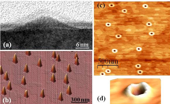
Fig. 1. Examples of the various types of nanostructures studied here: (a) TEM cross-section of a strain-induced InAs QD grown in Stranski–Krastanov mode. (b)3D AFM image of an AlGaAs surface with droplet epitaxial GaAs QDs. (c) Top view AFM image of an AlGaAs surface with nanoholes and GaAs quantum rings after local droplet etching with Ga. (d)3D AFM image of a nanohole with quantum ring.
Experimental data on the structural properties of the different nanostructures are collected in situ with reflection high-energy electron diffraction (RHEED) and ex situ with atomic force microscopy (AFM), transmission electron microscopy (TEM), and x-ray diffraction techniques. For an understanding of the basic physics behind the various self-assembly processes, we apply theoretical methods such as scaling analysis, Monte Carlo simulations, and coupled rate-equations. These studies provide a deep understanding of the influence of the process conditions and, thus, the ability to tailor the nanostructures structural properties.
Electronic and hole states confined inside semiconductor QDs exhibit a shell structure with states often denoted as s, p, d, … in analogy to atomistic nomenclature (although the respective confinements are different). The optical emission from these states is measured with photoluminescence (PL) spectroscopy (Fig. 2a). With single-dot PL spectroscopy we study the excitonic fine-structure of the QDs (Fig. 2b) which is important for instance in view of future applications in the fields of quantum computing or cryptography.
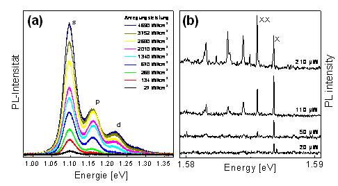
Fig. 2 (a) PL power series from an ensemble of InAs QDs grown in Stranski-Krastanov mode. Clearly visible at higher excitation power is the QD shell structure with s, p, d states. (b) Single-dot PL spectra from a GaAs QD fabricated by filling of a LDE nanohole. X denotes an excitonic peak and XX a biexciton. T = 4 K.
Transport measurements of QD systems are sensitive to electron or holes states, selectively, and to the influence of the Coulomb blockade. We perform capacitance-voltage (CV) and deep level transient spectroscopy (DLTS) on layers with self-assembled QDs embedded in Schottky-diodes. The DLTS spectra allow the determination of the timescale and mechanism for charge carrier escape from the QDs.
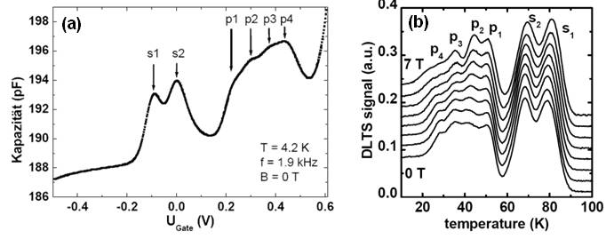
Fig. 3 (a) CV spectra from an ensemble of InAs QDs with two s and four p states. (b) DLTS spectra at varied magnetic field from InAs QDs.
Epitaxial Ferromagnet/Semiconductor Hybrids for Spintronics
Hybrid structures consisting of ferromagnets and modulation-doped semiconductor heterostructures are fabricated for Spintronic applications. Ferromagnetic metals, in particular Heusler alloys, possess electron systems with a high degree of spin polarization. For spintronic devices it is important to achieve a high spin-injection rate from the ferromagnet into the low-dimensional electron system of a semiconductor. The quality of the interfaces is crucial for polarized spin injection. Therefore epitaxially grow metallic layers on semiconductor heterostructures. The hybrid structures will be fabricated in an ultra-high vacuum cluster of semiconductor- and metal-deposition chambers. With this facility it is possible to deposit the metallic layer directly after the semiconductor growth without contact to air.
More details are here.
Mechanisms of Epitaxial Growth and Self-Assembly of Semiconductor Nanostructures
Coming soon ...